
THE WHITE RABBIT PROJECT
J. Serrano, M. Cattin, E. Gousiou, E. van der Bij, T. Włostowski, CERN, Geneva, Switzerland
G. Daniluk, AGH University of Science and Technology, Krakow, Poland
M. Lipi
´
nski, Warsaw University of Technology, Warsaw, Poland
Abstract
White Rabbit (WR) is a multi-laboratory, multi-
company collaboration for the development of a new
Ethernet-based technology which ensures sub-nanosecond
synchronisation and deterministic data transfer. The
project uses an open source paradigm for the development
of its hardware, gateware and software components. This
article provides an introduction to the technical choices and
an explanation of the basic principles underlying WR. It
then describes some possible applications and the current
status of the project. Finally, it provides insight on current
developments and future plans.
INTRODUCTION
The White Rabbit (WR) project [1] was initiated at
CERN in 2008 to start preparing the evolution of the Gen-
eral Machine Timing (GMT) system. The GMT is based
on uni-directional 500 kb/s RS422 links, and allows oper-
ators and other users to synchronise different processes in
CERN’s accelerator network. The system has a number of
shortcomings though, among which the most important are
the limited bandwidth and the impossibility of dynamically
evaluating the delay induced by the data links.
WR started with the following specifications:
• Transfer of a time reference from a central location to
many destinations with an accuracy better than 1 ns
and a precision better than 50 ps.
• Ability to service more than 1000 nodes.
• Ability to cover distances of the order of 10 km.
• Data transfer from a central controller to many nodes
with a guaranteed upper bound in latency.
One of the main aims of the project is to deliver the
above functionality while using – or extending where
needed – existing standards. Ethernet was chosen as the
physical layer for all data transmission. The most pre-
cise standard synchronisation method for Ethernet net-
works is the Precise Time Protocol (PTP), standardised as
IEEE 1588. With PTP it is possible to synchronise stations
with an accuracy in the order of 1 µs. WR extends PTP in
a backwards-compatible way to achieve sub-ns accuracy.
Figure 1 shows the layout of a typical WR network.
Data-wise it is a standard Ethernet switched network, i.e.
there is no hierarchy. Any node can talk to any other node.
Regarding synchronisation, there is a hierarchy established
by the fact that switches have downlink and uplink ports.
A switch uses its downlink ports to connect to uplink ports
of other switches and discipline their time. The uppermost
switch in the hierarchy receives its notion of time through
external TTL Pulse Per Second (PPS) and 10 MHz inputs,
along with a time code to initialise its internal International
Atomic Time (TAI) counter.
Figure 1: Layout of a typical WR network.
WR switches allow users to build highly deterministic
data networks by having different internal queues for Eth-
ernet frames of different priorities, as established by the
priority header defined in IEEE 802.1Q. The combination
of deterministic latencies and a common notion of time to
within 1 ns allows WR to be a suitable technology to solve
many problems in distributed real-time controls and data
acquisition. The following section describes the technolo-
gies used to cope with the synchronisation requirements in
WR.
TECHNOLOGIES
The three key technologies used in WR to achieve sub-ns
accuracy in synchronisation are PTP, layer-1 syntonization
and precise phase measurements. In the following para-
graphs, we describe each one in turn.
Precise Time Protocol
The IEEE 1588 standard specifies a way to evaluate the
link delay between two nodes – one master and one slave –
through the exchange of time-tagged messages. Figure 2
shows a simplified view of these exchanges.
The master node sends an initial message to the slave
and stamps it with a time-stamp t
1
as it goes out of its net-
working interface. The message is received at a time t
2
in
the slave’s time base. The process is then reversed, with
a new message sent from the slave at time t
3
and received
in the master at time t
4
. Assuming that the one-way delay
through the network is exactly half of the two-way delay
THBL2 Proceedings of IBIC2013, Oxford, UK
ISBN 978-3-95450-127-4
Copyright
c
○ 2013 by JACoW — cc Creative Commons Attribution 3.0 (CC-BY-3.0)
936 Time Resolved Diagnostics and Synchronization

Master
time
Slave
time
Announce
Sync
Delay_Req
Follow_Up
Delay_Resp
Management
t
1
t
2
t
3
t
4
Figure 2: Simplified PTP message exchange diagram.
– an assumption which is never completely accurate – the
one-way delay can be estimated as:
δ =
(t
4
− t
1
) − (t
3
− t
2
)
2
(1)
Typical PTP implementations use free-running oscilla-
tors in each node. This means that there will be a grow-
ing time drift between master and slave unless the message
exchange and calculation of δ happen repeatedly. Even if
there is such a continuous exchange of messages, the time
bases will drift during the time interval between two cal-
culations of δ. WR nodes extract the clock signal from the
incoming data stream, through a mechanism called “layer-
1 syntonization”. This results in equal clock frequencies in
all nodes, therefore eliminating the drift problem present in
typical PTP implementations.
Layer-1 Syntonization
In WR, as in the ITU-T Synchronous Ethernet standard,
the mechanism used to guarantee that all nodes are clocked
at the same frequency works at the level of the physical
layer, with no impact whatsoever on data traffic. WR cur-
rently supports Gigabit Ethernet (GbE) on fibre only. In
GbE, the link is never idle. Even if a node has nothing to
transmit, its Medium Access Control (MAC) block gener-
ates special 8B10B patterns called commas, whose purpose
is to avoid unlocking of the Phase Locked Loop (PLL) on
the Clock and Data Recovery (CDR) circuit in the receive
(RX) path of the node connected to it. Commas also help
in aligning the serial-to-parallel converter on the receiving
node.
Figure 3 depicts the mechanism of layer-1 syntoniza-
tion. In standard Ethernet, each node uses its own free-
running clock to encode the messages it sends to the node
on the opposite side of the link. By contrast, a network
using layer-1 syntonization establishes a clocking hierar-
chy, whereby there is one master node or switch. All other
nodes and switches extract their clock signals from data
streams, in such a way that all of the system clocks of nodes
and switches on the network end up beating at exactly the
same rate. Switches play a key role in this frequency distri-
bution, by extracting the clock from the data stream going
into one of their ports (uplink port) and using that extracted
clock in the encoding of all data streams going out of all
ports (uplink and downlinks).
Figure 3: Simple illustration of layer-1 syntonization.
Precise Phase Measurement
As we saw in the preceding paragraph, a downlink port
of a switch disciplines the frequency of a downstream
switch by connecting to its uplink port. The downstream
switch, in turn, uses this extracted clock to encode the data
which it sends back to the upstream switch. In this way, the
upstream switch finds a delayed copy of its encoding clock
in the output of the CDR circuit in its RX path, as depicted
in Fig. 4. The phase shift between these two clock signals
is directly related to the link delay, and a measurement of
this phase difference can therefore be incorporated into the
PTP equation in order to achieve better precision.
Figure 4: Phase tracking block diagram.
In addition, a phase-shifting circuit can be included in
the slave node to create a phase-compensated clock signal,
i.e. a clock signal which is in phase with the master clock
signal despite the delay introduced by the fibre link. The
delay programmed into this phase shifter at any given time
is of course taken into account when calculating the link
delay.
The introduction of layer-1 syntonization and phase
tracking provides a synchronisation mechanism which can
potentially be completely independent of the data link
layer. Beyond the first PTP message exchange, there is in
principle no need to continue exchanging messages to keep
the nodes synchronised. In practice, WR keeps the PTP
messages going for robustness reasons, albeit at a much re-
duced rate. This makes the PTP traffic negligible in terms
Proceedings of IBIC2013, Oxford, UK THBL2
Time Resolved Diagnostics and Synchronization
ISBN 978-3-95450-127-4
937
Copyright
c
○ 2013 by JACoW — cc Creative Commons Attribution 3.0 (CC-BY-3.0)

of bandwidth, therefore not getting in the way of determin-
ism for the user frames, another key requirement for WR.
Layer-1 syntonization also allows to cast the time-
stamping problem into a phase measurement problem,
which increases precision since phase measurement can be
done much more precisely than measuring time intervals.
The circuit we use for measuring phases, called Digital
DMTD (Dual Mixer Time Difference), is depicted in Fig. 5.
Figure 5: Digital DMTD circuit.
The flip-flops (FFs) in this digital implementation play
the role of the mixers in the original DMTD circuit [2].
This circuit measures the phase difference between two
clock signals, clk
A
and cl k
B
, which have the same nom-
inal frequency. A PLL is used to generate a third clock
signal, very close but not quite at the same frequency as
clk
A
and clk
B
. The FFs sample the two incoming signals
with this synthesised clock signal. Since the sampling fre-
quency is very close to that of the incoming signals, very
low frequency waveforms result at the outputs of the FFs.
There are some glitches in the edges of these low-frequency
square waves as a result of the very slow sweeping and the
jitter in the incoming signals. The slow sweeping – equiva-
lent to the low-frequency beat in the analogue version of the
circuit – provides a magnifying effect. Tiny phase differ-
ences in the input signals become readily measurable time
intervals after sampling and cleaning up the glitches. The
circuit is fully digital and extremely linear. This circuit is
used as a phase detector in the master and as part of the
phase shifter in the slave. Indeed, one can build a very
linear phase shifter by using this phase detector in a loop,
and having a non-linear phase shifter shift the phase until
the linear phase detector signals the nominal phase shift is
attained.
THE WHITE RABBIT SWITCH
WR is a switched network. At its heart lies its most
important component: the WR switch, which provides 18
ports in a 1U 19” rackable enclosure. It is made of open
source hardware, gateware and software, and it is sold and
supported by a commercial company. WR switches are
fully compatible with Ethernet, and can identify if a WR
node or another WR switch is hooked to one of their ports
by using the WR extension [3] to the IEEE 1588 protocol
at link establishment time. This extension is also designed
to be backwards-compatible with standard PTP, so it is pos-
sible to connect existing PTP gear to a network made with
WR switches, along with WR nodes. In this case, the WR
nodes will benefit from the extension and therefore achieve
better accuracy, while the standard PTP nodes will run only
the standard protocol and feature reduced accuracy.
Architecture
Figure 6 shows a high-level block diagram of the WR
switch. Ethernet frames are exchanged through 18 ports
equipped with Small Form-factor Pluggable (SFP) sockets
which can host optical transceivers. The reference imple-
mentation uses SFP modules for one single mode fibre, us-
ing one wavelength for TX traffic and a different one for
RX. The use of a single fibre ensures that the symmetry in
TX and RX paths – after mathematically compensating for
fibre dispersion – is robust, in particular against changes in
cabling not notified to the final user. The SFPs are con-
nected directly to a Xilinx Virtex-6 Field Programmable
Gate Array (FPGA).
Figure 6: High-level block diagram of the WR switch.
Ethernet frames get switched inside the FPGA with very
low latency. An ARM CPU running Linux helps with
less time-sensitive processes like remote management and
keeping the frame filtering database in the FPGA up to date.
The clocking resources block contains PLLs for cleaning
up and phase-compensating the system clock, as well as
for generating the frequency-offset DMTD clock.
FPGA Design
Figure 7 shows a block diagram of the internals of the
FPGA in the switch. Blocks under development are shown
in white boxes with grey borders, and will be discussed
in another section. The current release, without those
blocks, is fully operational. The design consists of Hard-
ware Description Language (HDL) cores around a Wish-
bone bus [4] interconnect.
There are 18 Endpoint blocks, each connected to an SFP
in the switch. They send and receive Ethernet frames using
the switching core (SwCore) to communicate with one an-
other. The decision as to where a frame is destined is taken
by a forwarding process in the Routing Table Unit (RTU).
THBL2 Proceedings of IBIC2013, Oxford, UK
ISBN 978-3-95450-127-4
Copyright
c
○ 2013 by JACoW — cc Creative Commons Attribution 3.0 (CC-BY-3.0)
938 Time Resolved Diagnostics and Synchronization
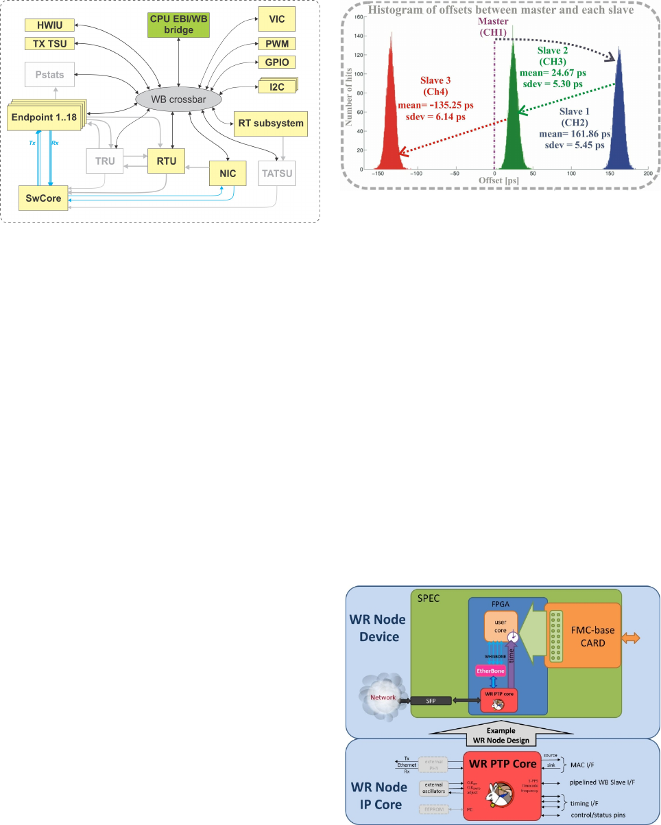
Figure 7: Block diagram of the FPGA design in the WR
switch.
The choice of the word “routing” here is a bit unfortunate
since we are speaking about layer-2 forwarding, not layer-3
routing.
All traffic to and from the ARM CPU goes through the
CPU EBI/WB bridge. This interface is e.g. used to keep the
database up to date in the RTU. The ARM CPU itself can
be a source or sink for Ethernet frames, using the Network
Interface Card (NIC) and the Vector Interrupt Controller
(VIC) blocks in the FPGA. The ARM CPU also runs the
PTP stack for the switch, and reads the time stamps for
outgoing frames from the TX Time Stamp Unit (TX TSU).
The Real Time (RT) subsystem block is responsible
for timekeeping in the switch. It contains an LM32 soft
CPU running a soft PLL which controls the various pro-
grammable oscillators in the switch. In addition, it hosts
the counters for the current TAI.
The Hardware Info Unit (HWIU) contains important in-
formation about the global HDL design itself, such as the
HDL commit hash in the Git repository and the date of the
synthesis. The I2C, GPIO and PWM blocks control other
peripherals on the switch, such as LEDs and the cooling
fans.
Performance
In order to characterise the performance of the WR
switches, a system was set up in a laboratory consisting of
four cascaded WR switches. The master switch was con-
nected to a first slave switch through a 5 km fibre roll. Sim-
ilar fibre rolls were used to connect the first switch to the
second one, and then the second one to the third one, for a
total of 15 km of fibre. Adverse conditions were simulated
by heating the fibre rolls with a hot air gun.
Since the four switches were all in the same laboratory, it
was easy to monitor their PPS outputs with an oscilloscope
and draw histograms of the offsets between the PPS output
in each switch and the PPS output in the master switch. The
results of these measurements can be seen in Fig. 8.
As can be seen in the plots, accuracy always stays within
± 200 ps, and typical precisions are in the order of 6 ps.
Figure 8: Histograms of PPS output offsets of three cas-
caded WR switches with respect to the PPS pulse output in
the master switch.
The same type of accuracy and precision is found with WR
nodes, since the technologies involved for delay measure-
ment and compensation are exactly the same as those used
in the switches.
WHITE RABBIT NODES
Figure 9 shows a simplified block diagram for a WR
node based on the Simple PCI Express Carrier (SPEC)
board [5]. This card can host mezzanines conforming to the
FPGA Mezzanine Card (FMC) VITA 57 standard. We have
developed Analogue to Digital Converter (ADC), Time-to-
Digital Converter (TDC) and programmable delay genera-
tor FMCs. By plugging these cards in a WR-enabled car-
rier such as the SPEC, and appropriately configuring the
FPGA in the carrier board, one can enhance their function-
ality with features such as synchronous sampling clocks in
remote nodes and precise TAI time stamps.
Figure 9: An example WR node.
In order to enable users to easily build nodes for WR-
based applications, we have developed a core which takes
care of all WR data transmission and reception, along with
all synchronisation tasks. This WR PTP Core (WRPC) [6]
Proceedings of IBIC2013, Oxford, UK THBL2
Time Resolved Diagnostics and Synchronization
ISBN 978-3-95450-127-4
939
Copyright
c
○ 2013 by JACoW — cc Creative Commons Attribution 3.0 (CC-BY-3.0)

– an Ethernet Medium Access Control (MAC) unit with en-
hancements for timing – contains an LM32 soft CPU inside
which runs the whole PTP stack. Frames which are iden-
tified as non-PTP are forwarded downstream to the user
logic. Conversely, the core also accepts frames from user
logic, which can for example be used to stream data ac-
quired in an ADC FMC. The WRPC takes care of control-
ling the programmable oscillators on the SPEC or any other
WR-enabled board. An Etherbone slave core [7] can op-
tionally be instantiated between the WRPC and the user
logic. Etherbone is an independent project led by GSI
which can work in conjunction with any Ethernet MAC
core, not necessarily with the WRPC. It aims at provid-
ing a way to trigger reads and writes in a remote Wishbone
bus through carefully defined payloads in an Internet Pro-
tocol (IP) packet. With Etherbone, a complete network of
sensors and actuators looks like a big memory map to a
master/management node.
WR-capable nodes have been designed in PCIe, PXIe,
VME64x and µTCA form factors. These designs have
varying degrees of maturity and commercial support. The
most mature one is the PCIe SPEC board, and different
WR-based gateware designs have been successfully tar-
geted at it, including a Network Interface Card with a Linux
network device driver.
APPLICATION EXAMPLES
WR technology provides users with a common notion
of TAI in every node and with a deterministic network in
which an upper bound for latencies is guaranteed by design.
This opens up many possibilities in different fields, such as
Multiple Input Multiple Output (MIMO) feedback systems.
In this section, we describe just two of the multiple possible
applications of WR.
RF Distribution
WR distributes a 125 MHz clock – typically TAI-
related – for free. A WR user gets access to this clock, or
derivatives of it, just by hooking a WR node to a WR net-
work. However, in some cases users care more about syn-
chronising to Radio Frequency (RF) signals related to e.g.
the accelerating structures in a particle accelerator. Gener-
ating phase-compensated RF signals in different locations
can be useful in other domains as well, such as in radar
applications.
Figure 10 shows a block diagram of how one can use
a WR network to distribute RF clocks, through a scheme
called Distributed Direct Digital Synthesis (Distributed
DDS or D3S).
The reference clock line in the drawing is just concep-
tual. Nodes get the reference clock from the WR network
itself. There is no need for additional connections. The
transmitting node tracks an RF signal connected to its in-
put with a PLL in which the role of the voltage-controlled
oscillator is fulfilled by a DDS block. The control words
for that DDS, along with the TAI at which they were ap-
plied, are encoded and broadcast through the WR network.
Figure 10: Distributed DDS in a WR network.
Receiving nodes can then apply a fixed offset to the TAI
stamps and replay the RF waveform with their local DDS
blocks, with just a fixed delay. In most situations the RF is
stable enough for this fixed delay to be of no concern.
This scheme has several advantages over traditional RF
distribution systems. There is no additional cabling to
be done. The same network can handle more than one
distributed RF. In addition, all waveforms are played us-
ing a TAI-related clock, which is very useful for diagnos-
tics. A first crude implementation has been demonstrated
at CERN, with a jitter – defined here as the integral of the
Power Spectral Density of the phase noise, integrating be-
tween 10 Hz and 5 MHz – in the replayed RF below 10 ps.
Better jitter can be achieved by carefully tuning the digi-
tal PLL filter and cleaning the output of the DDS with an
analogue PLL including a low phase noise oscillator.
Distributed Oscilloscope
Figure 11 shows a conceptual representation of a dis-
tributed oscilloscope using several of the building blocks
we have described so far.
Figure 11: Distributed oscilloscope using a WR network.
ADC nodes sample analogue signals synchronously in
remote locations. The synchronous phase-compensated
sampling is facilitated by the WR-derived clock. The
ADCs can store their samples in rolling buffers, where each
location is known to contain the sample corresponding to a
precise TAI. As soon as an ADC node detects a condition
upon which it should trigger, it can broadcast a trigger mes-
sage through the WR network. All nodes will have received
that message after a guaranteed worst-case delay. These
nodes can then stop sampling and rewind their buffers to
the TAI specified in the triggering message. External trig-
ger pulses can also be accommodated through the use of
TDC nodes, and sampling with non-TAI-related clocks can
be done using D3S nodes.
THBL2 Proceedings of IBIC2013, Oxford, UK
ISBN 978-3-95450-127-4
Copyright
c
○ 2013 by JACoW — cc Creative Commons Attribution 3.0 (CC-BY-3.0)
940 Time Resolved Diagnostics and Synchronization

A computer in the control room then gets all the TAI-
stamped acquisition data and displays it coherently on a
single screen. The operators then see this whole distributed
system as a simple oscilloscope to which all their signals
are connected. This would of course be impossible with
a real oscilloscope, but it can be done with WR’s phase-
compensated distribution of TAI, appropriate WR-enabled
nodes and software.
THE WR COMMUNITY
The WR project is a distributed endeavour whose collab-
orative model is heavily inspired by that typically used in
Free/Open Source software projects. All the intermediate
and final results in the project are made available through
open source licences. We use mostly the GNU General
Public License (GPL) and the GNU Lesser General Public
License (LGPL) for licensing software, LGPL for gateware
(HDL files) and the CERN Open Hardware Licence [8] for
hardware designs.
WR users are very often developers and vice versa. The
ever-growing list of interested institutes and companies [9]
has enlarged the scope of the project well beyond the origi-
nal domain of particle accelerators. At CERN, the effort of
dissemination for this technology has been coordinated in
collaboration with the Knowledge Transfer Group.
Thanks to its open nature, the project has benefited from
extensive contributions and ideas of potential and con-
firmed users. These exchanges typically happen on the
project mailing list, which is web-archived and integrated
with the project website [1]. Peer review over email or in
dedicated workshops establishes a meritocracy in which the
best ideas move forward. Openness is also key in avoiding
potential vendor lock-in situations and welcoming com-
mercial partners as any other contributor.
PROJECT STATUS AND OUTLOOK
At the time of this writing (August 2013) the WR switch
is a mature commercially-supported hardware product with
a stable release for its gateware and software. WR nodes
have been designed and validated in a variety of formats,
and they have consistently shown sub-ns synchronisation
accuracy. This section provides a quick overview of some
of the most important upcoming efforts in the project.
Synchronisation Performance
The results in Fig. 8 show that the original goals for WR
in terms of synchronisation have been achieved. In some
applications though, it is important to improve accuracy as
much as possible. While the WR delay model [10] and
compensation mechanism cover changes in fibre temper-
ature appropriately, they do not compensate for the delay
fluctuations induced by temperature variations in the nodes
and switches themselves. We believe these effects can ac-
count for tens of picoseconds or even more in particularly
adverse circumstances.
Tests in a climatic chamber [11] have shown that the de-
pendency of delay with respect to temperature is mostly
linear, so an evolution of the WR delay compensation algo-
rithm which takes into account on-board temperature mea-
surements should help in this respect. The modified algo-
rithm could include a linear model of the dependency or a
table of delay vs. temperature values resulting from offline
calibration.
Switch Evolution
The efforts on switch gateware and software will go in
the direction of providing better support for remote man-
agement, diagnostics and robust data transmission in a WR
network.
A Port Statistics block (Pstats, see Fig. 7) will be added
to provide counts of transmitted, received and dropped
frames per port, along with other counts relevant for as-
certaining the state of health of the network. A Time-
Aware Traffic Shaper Unit (TATSU) will allow blocking
selected output queues for some time so that high-priority
frames can go through the switch without colliding with
low-priority frames being sent at that moment through a
port. This will avoid having to wait until the end of trans-
mission of those frames before taking ownership of the
port.
In addition, a Topology Resolution Unit (TRU) will
add hardware support to the process of providing redun-
dant loop-free topologies for a network. This will result
in a faster topology switch-over compared to traditional
software-based methods such as the Rapid Spanning Tree
Protocol (RSTP). Figure 12 illustrates why fast switch-over
can be important in a WR network.
Figure 12: Forward Error Correction used to correct for
frame loss.
In this example, a WR node decomposes a control mes-
sage into four Ethernet frames which have been encoded
using Forward Error Correction (FEC), in such a way that
receiving any two of those frames allows the receiving node
to re-constitute the original control message. The use of
this type of FEC scheme is well adapted to networks in
which a late frame is a wrong frame, such as the one used
for accelerator timing at CERN. This precludes the use of
protocols which require re-trials in case of transmission er-
rors, such as the Transmission Control Protocol (TCP).
If the switch can enable a redundant port very quickly
after detecting a fatal condition in another port, and if the
switch-over time is lower than that corresponding to the
transmission of one of the frames in the figure, the receiv-
ing node will be able to re-constitute the message with the
remaining frames. Tests at CERN have shown that this kind
Proceedings of IBIC2013, Oxford, UK THBL2
Time Resolved Diagnostics and Synchronization
ISBN 978-3-95450-127-4
941
Copyright
c
○ 2013 by JACoW — cc Creative Commons Attribution 3.0 (CC-BY-3.0)

of switch-over speeds are indeed possible with appropriate
hardware support.
On the software front, most of the activity will be fo-
cused on providing the switch with good Simple Network
Management Protocol (SNMP) support so that all control
and diagnostics can happen remotely using standard switch
management software. Another important development
will be the replacement of the current PTP stack running
in the ARM processor by the PTP Ported to Silicon (PPSi)
stack. PPSi [12] is a portable PTP daemon which can be
targeted at bare-metal systems, such as the LM32 proces-
sor inside the WRPC in the WR nodes, but can also run
under an operating system, such as the Linux running in
the ARM processor in the switch. PPSi has been devel-
oped in the frame of the WR project but can be used in any
project requiring PTP support. It is licensed under LGPL.
Standardisation
Using standards is good for many reasons. A standard is
more likely to be used for a long time, so using it reduces
long-term risks. Standardisation bodies typically invest a
big effort in making sure standards are robust, so adopting
them also saves time. Finally, companies are more inclined
to participate in a development project if it is based on stan-
dards, because markets are typically larger in that case and
also because the rules of governance and evolution of the
standard are clear from the outset.
In WR, we are developing functionality which is not
made available by any existing standard. However, it
was felt from the beginning of the project that WR ideas
could constitute the basis for the evolution of the IEEE
1588 standard. The original WR specification was already
worded with this in mind. Now the IEEE P1588 Working
Group [13] has opened the process for the periodic revi-
sion of the standard, and the WR project is represented in
the subcommittee for high accuracy enhancements. The
aim of this effort for the WR team is to end up in a situ-
ation where WR is just a particularly accurate and precise
implementation of the IEEE 1588 standard. The work of
the subcommittee has just started, and the outlook is very
promising.
WR is also concerned with determinism, and the WR
team keeps an eye on the efforts of the Time Sensitive Net-
works (TSN) Task Group [14] inside the IEEE 802.1 Work-
ing Group. The ideas discussed in this Task Group are of
great relevance to WR. Conversely, the TRU and TATSU
blocks in Fig. 7 can be a very convenient testing ground for
these ideas.
ACKNOWLEDGEMENT
The authors acknowledge the contribution of the WR
community at large for collaborating in the development
of the technology, identifying and reporting bugs and ex-
tensively testing each release of hardware, gateware and
software. Authorship of this paper does not imply a claim
to more importance inside the project, but rather a privilege
to report on the results of the collective effort of the many
contributors to the project.
REFERENCES
[1] White Rabbit project website,
http://www.ohwr.org/projects/white-rabbit/wiki.
[2] D.A. Howe et al,. “Properties of Signal Sources and Mea-
surement Methods,” Proceedings of the 35
th
Annual Sym-
posium on Frequency Control, (1981).
[3] M. Lipi
´
nski et al., “White Rabbit: a PTP Application for
Robust Sub-nanosecond Synchronization,” ISPCS 2011.
[4] Wishbone bus specification,
http://opencores.org/opencores,wishbone.
[5] Simple PCI Express Carrier website,
http://www.ohwr.org/projects/spec/wiki.
[6] WR PTP Core, http://www.ohwr.org/projects/
wr-cores/wiki/Wrpc core.
[7] Etherbone Core project,
http://www.ohwr.org/projects/etherbone-core/wiki.
[8] CERN Open Hardware Licence,
http://www.ohwr.org/cernohl.
[9] WR users, http://www.ohwr.org/projects/
white-rabbit/wiki/WRUsers.
[10] White Rabbit Specification,
http://www.ohwr.org/documents/160.
[11] WR torture report,
http://www.ohwr.org/documents/190.
[12] PPSi,
http://www.ohwr.org/projects/ppsi/wiki.
[13] IEEE P1588 Working Group,
https://ieee-sa.centraldesktop.com/1588public.
[14] Time-Sensitive Networks Task Group,
http://www.ieee802.org/1/pages/tsn.html.
THBL2 Proceedings of IBIC2013, Oxford, UK
ISBN 978-3-95450-127-4
Copyright
c
○ 2013 by JACoW — cc Creative Commons Attribution 3.0 (CC-BY-3.0)
942 Time Resolved Diagnostics and Synchronization
